

The Bosch Wafer Fab in Dresden, Germany is touted as the world’s most modern.
Deepti Thore looks at the capabilities of the smart, future-ready factory.
The automotive industry, globally, is finding ways to overcome the shortage of semiconductors. In effect, even with demand sentiment improving, these big supply-side constraints are the biggest handicap for automotive Original Equipment Manufacturers (OEM). It is feared to continue to negatively impact growth for the rest of the fiscal. For a semiconductor, wafers are the key input raw material. After all, it is on these wafers that fabrication with a series of repeated sequential steps aid in the production of electronic circuits on the semiconductor wafer.
Bosch is among manufacturers looking at capacity expansion and key acquisitions to ease the bottleneck that is nothing short of a crisis. Dr Volkmar Denner, Chairman of the Board of Management, Robert Bosch GmbH, in a company release claims, “In Dresden, with the help of artificial intelligence, we will take semiconductor manufacturing to the next level.” In June 2021, the company had announced the inauguration of Bosch Wafer Fab in Dresden, Germany. Touted as the world’s most modern wafer fabrication labs. The smart, future-ready factory is claimed to be fully connected, data-driven, and notably capable of self-optimising. At the factory, the integrated processes coupled with Artificial Intelligence (AI) sets a new benchmark for industry 4.0 manufacturing as per Denner. “The new wafer fab is the single largest investment in the company’s history. This cannot be stressed too much. Its size and additional production capacity alone are impressive. The very latest methods of data-driven continuous improvement in production make the Dresden plant a smart factory. To put it another way: in this plant, natural and artificial intelligence have joined forces with the internet of things to form a productive symbiosis,” he mentions.
Smart manufacturing
Automotive chips are special grade chips. Subjected to varied and challenging operating conditions in different terrains and in suboptimal conditions, they require special expertise. As chips must meet higher standards of reliability, it translates to the development of automotive semiconductors being more complicated than in other applications. This requires specialist expertise, and Bosch is backing itself. Harald Kroeger, Member of the Board of Management of Robert Bosch GmbH, explains, “This dual strength – the combination of chip and systems expertise – is strategically important for Bosch.” Through the new wafer fab, Bosch will continue to ensure product quality, and continuous refinement at reduced costs in line with the self-optimising capabilities of the smart, future-ready factory.

With an estimated investment of one billion euros, the new wafer fab will put to use a comprehensive IT system including multiple server-driven, computer-controlled manufacturing systems riding high on automation. The applications benefit from a connected infrastructure operating at 5G speeds for a quicker turnaround and exchange of information. Wafer fabrication is expected to commence in September 2021 and is expected to boost the availability of semiconductors. “The new Bosch wafer fab will boost our capacity in microelectronics. Microelectronics is the basis for nearly every promising technology, for applications of artificial intelligence, for quantum computing, and for automated and connected driving – which is also a Bosch speciality,” stated Chancellor of the Federal Republic of Germany, Dr Angela Merkel on the sidelines of the inauguration. ACI
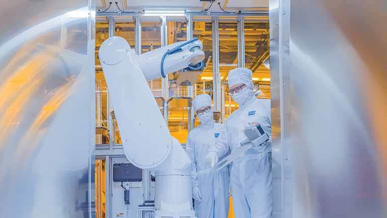
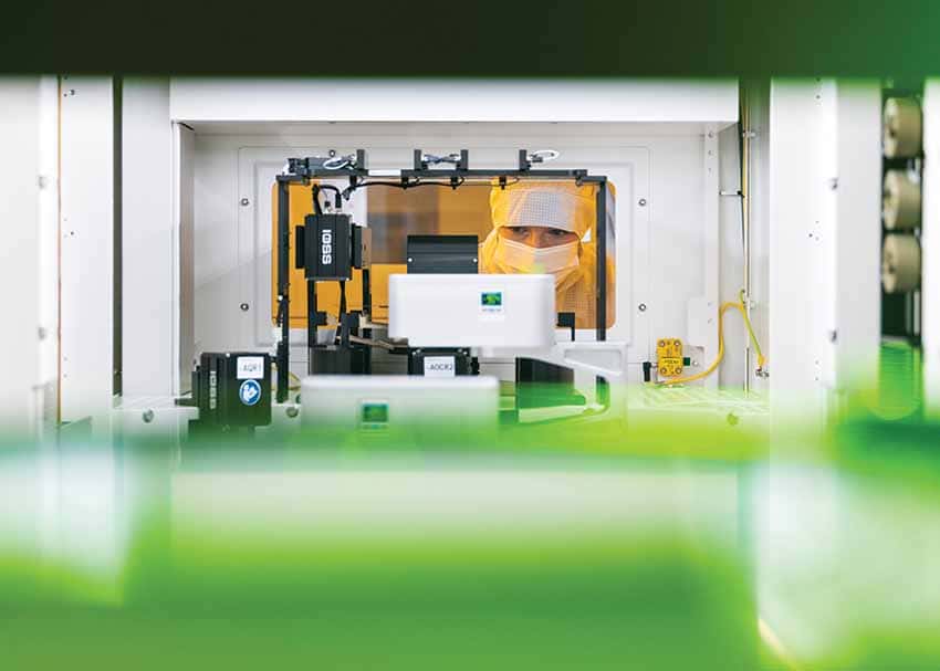
Wafer Fabrication
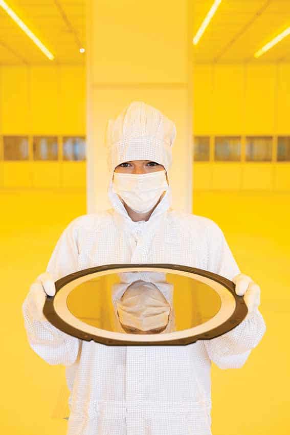
Just 60 µm thick, the 300 mm silicon discs are the key input material for the semiconductor chips. In a six-week production process, these finished wafers accommodate 31,000 individual chips. “Our new wafer fab sets standards in automation, digitalisation, and connectivity,” cites Harald Kroeger, Member of the Board of Management of Robert Bosch GmbH. Known to be light-sensitive, it requires the chips to be developed in a highly isolated environment. The wafers are handled in an end-to-end automated fabrication process which is a USP of the factory. An autonomous conveyor system manoeuvres the wafers from one station to the other. Using multi-axis robotic arms, the wafers are dipped in specialised liquid formulations followed by colossal microscopes scanning them independently at the end of the production line. An AI-powered algorithm is said to detect even the slightest imperfections including image inspections, and scans of wafer signatures. To produce the semiconductor chips, the untreated or “bare” wafers are then processed for several weeks.